About Center for VLSI Design (CVD)
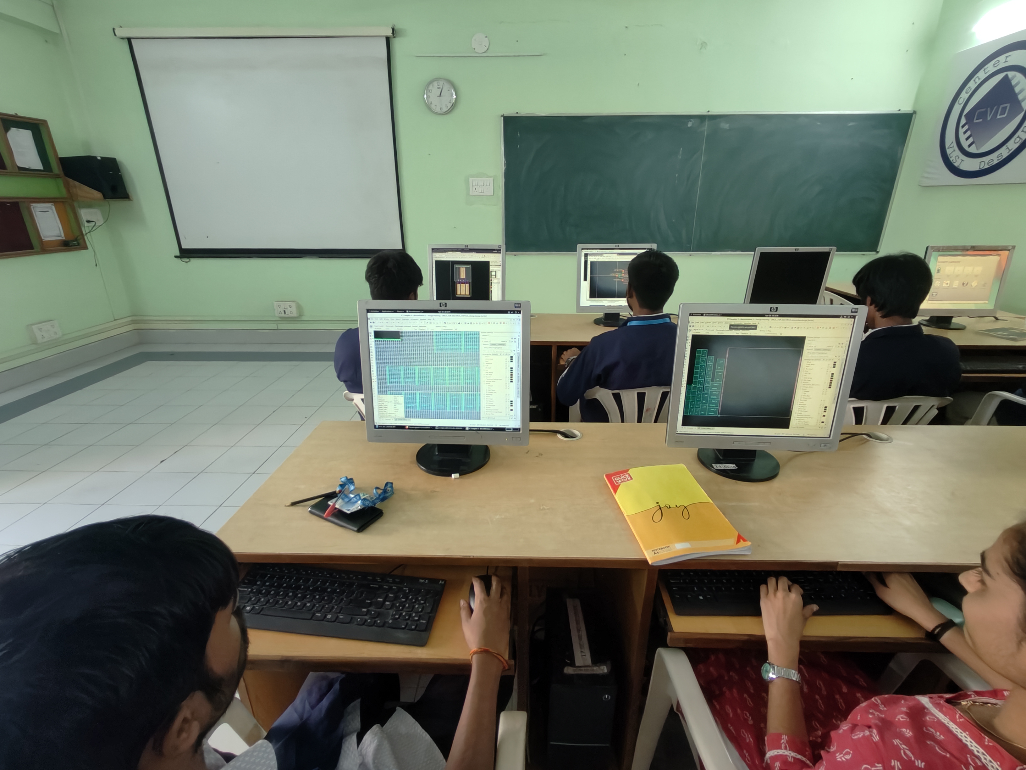
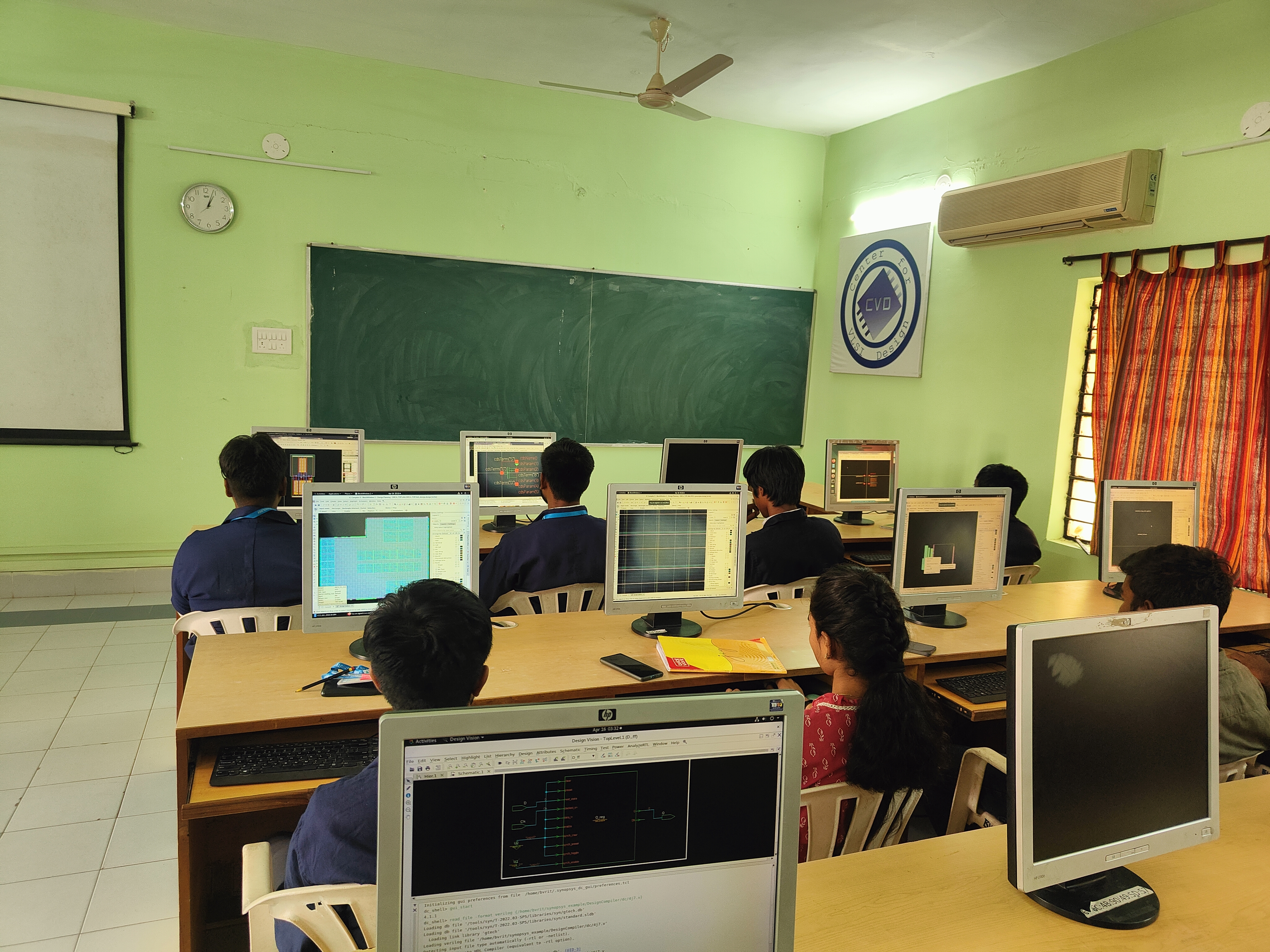
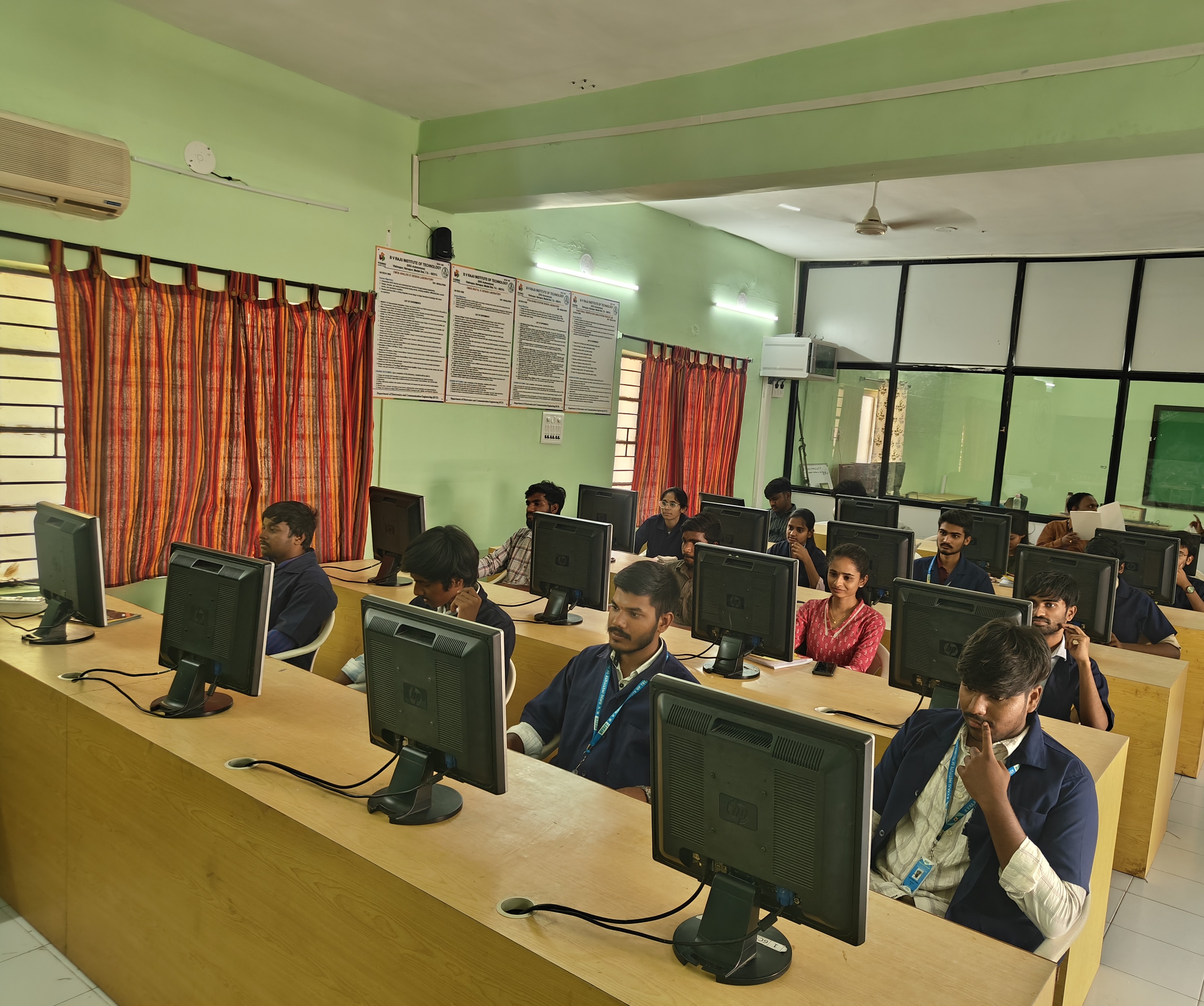
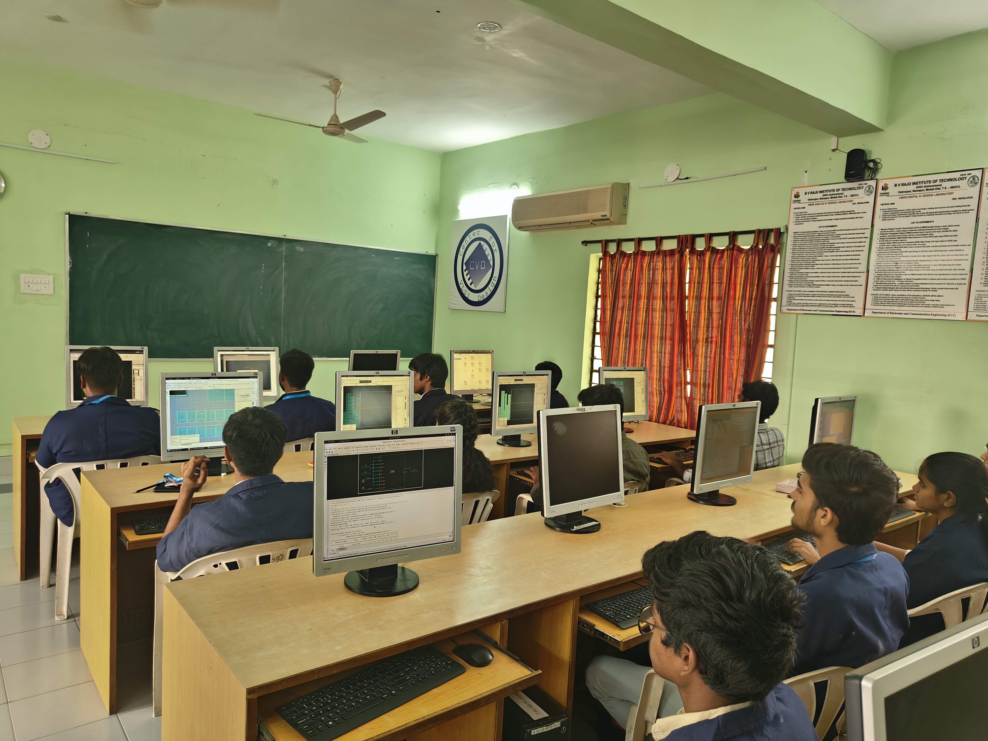
The Electronics and Communication Engineering established the Center for VLSI Design (CVD) in 2008. The CVD focuses specifically on Digital ASIC design, Analog and Mixed-signal and SOC VLSI design. The Objective of this center is to create an academic center of excellence in semiconductor technologies such as RTL, verification, physical design, DFT and Analog layouts. The key activities of the above center is to provide domain training by VLSI experts from Industry to Undergraduate and Post-Graduate students supported by CVD faculty members. The center also leans heavily on professional interactions with industry for guidance and support. The CVD associated with few VLSI companies like SYNOPSYS, XILIX, CYIENT, ADEPTCHIPS, MANJEERA DIGITAL SYSTEMS and HYSOC etc to provide training to the UG/PG students in VLSI domain. More than 140 students got placed in VLSI companies during the last six years.
We welcome the industries to collaboration for the benefit of our faculty and students; and also to bridge the gap between the Industry and Academia. This will surely be helpful for our students to choose their future career in the core Industry.
Objectives
- To Full fill the VLSI Industry-Academia Gap
- Hands on expose on ASIC and FPGA tools which includes Analog Design and Layout also.
- Final goal of CVD is to develop an Integrated circuit (IC) from BVRIT.
CVD Coordinator

CVD Team Members


CENTER FOR VLSI DESIGN
Department of Electronics and Communication Engineering
DETAILED SCHEDULE – AY: 2026-27
- Combinational Circuits:
S.NO | Sessions | TOPIC |
1 | Session-1 | Introduction to Logic Gates |
Multiplexers, Decoder | ||
Design of combinational circuits Using Multiplexers and Decoders | ||
Demultiplexers, Encoder, Comparators | ||
2 | Session-2 | Adders (Half Adder, Full Adder, Parallel Adder) &Substractor (HA,FA) |
Carry Look Ahead Adder, Full Adder Implementation using Decoders AND MUX | ||
K-Maps: Prime Implicants, Essential Prime Implicants, Hazards, Clock Skew. | ||
PAL, PLA, Function Implementation. | ||
3 | Session-3 | Introduction to VCS tool Basic Verilog Programming for Combinational Circuits: Behavioral Modeling and Test Benches on VCS |
4 |
Session-4 | 1: Verilog Implementation of Logic Gates 2: Multiplexers, Demultiplexers |
5 |
Session-5 | 3: Encoder, Decoder 4: Adders and Comparators. |
Tools: Synopsys-VCS
- Sequential Circuits:
6 | Session-6 | Latch & Flip Flops, Characteristic Equation, Excitation and Truth Tables. Master Slave JK F/F and Race Around Condition Flip Flop Conversions Shift registers, Universal Shift Register. Counters: Shift Register Based Counters.Asynchronous, Ripple Counters. |
7 | Session-7 | FSM: Mealy and Moore Machine, State Diagram, Sequence Detector Implementation using Mealy and Moore |
8 | Session-8 | Basic Verilog Programming for Sequential Circuits: Flip Flops, Synchronous and Asynchronous Circuits. |
9 | Session-9 | Basic Verilog Programming for 1: Registers 2: Counters |
10 | Session-10 | FSM: Mealy and Moore Machine Design with example. Sequence Detectors |
Tools: Synopsys VCS
S.NO | Sessions | TOPIC- Synthesis & Physical Design |
1 | Session-1 | · Industry Approach for VLSI Front-End Design Problems |
2 | Session-2 | · Clock Domain Crossing |
3 | Session-3 | · RTL Design Issues in Real Time |
4 | Session-4 | · Performing CDC Verification |
5 | Session-5 | · STA Concepts |
6 | Session-6 | · STA using Prime Time |
7 | Session-7 | · Physical Design Concepts |
8 | Session-8 | · Clock tree synthesis |
9 | Session-9 | · Physical design using ICC/ICC2 |
10 |
| · FIFO design Assignment |
Tools: Synopsys-Synthesis- DC compiler
STA-Primetime
Physical Design- ICC2
S.NO | Sessions | TOPIC |
1 | Session-1 | · Digital Design Concepts · Introduction to FIFO · RTL for FIFO |
2 | Session-2 | · Synthesis Concepts with DFT |
3 | Session-3 | · Synthesis Concepts with DFT |
4 | Session-4 | · Synthesis using Design compiler |
5 | Session-5 | · ATPG using Tetramax |
II.CMOS Digital and Analog IC Design:
6 | Session-6 | · Basic concepts on CMOS. · Introduction to Custom IC designer |
7 | Session-7 | · Implementation of logic gates using C-designer (transient and DC analysis) |
8 | Session-8 | · Implementation of differential op-amp using C- Designer (Power analysis) |
9 | Session-9 | · Basic concept of Layout design rules |
10 | Session-10 | · Layout design for logic gates using c-designer |
11 | Session-11 | · Mini project |
S.NO | Name of the Company | Date of MOU | Duration(Yrs) | Nature of MOU |
1 | Innominds | 05-09-2025 | 3 | To provide technology exposure, internships & Core Placements |
2. | STEM ROBOTICS | 29-07-2025 | 3 | To provide technology exposure, internships & Core Placements |
3 | Qubitsemi solutions | 03-07-2025 | 3 | To provide technology exposure, internships & Core Placements and consultancy |
4 | Krisemi | 01-02-2025 | 3 | To provide technology exposure, internships & Core Placements |
5. | UNIMAP | 04-10-2024 | 3 | Faculty exchange, collaboration for projects |
6 | Pennstate University | 10-02-2023 | 3 | Exchange of Teaching and research |
7 | Synopsys | 08-09-2023 | 3 | To provide technology exposure, internships & Core Placements |
8 | HEAMAC | 04-01-2023 | 3 | To provide technology exposure, internships & Core Placements |
9 | BITSILICA | 28-02-2023 | 3 | To provide technology exposure, internships & Core Placements |
10 | Maven silicon | 17/06/2021 | 3 | To provide technology exposure, internships & Core Placements |
11 | Dhruva Space PVT Ltd | 18/11/2019 | 3 | Training and R&D |
12 | National Instruments | 29/1/2019 | 3 | To provide technology exposure |
13 | Ferventz Technologies | 03/11/2018 | 3 | Training , Internships & Placements |
14 | Hysoc Technologies | 16/12/2017 | 3 | To provide technology exposure, internships & Core Placements. |
15 | Corel Technologies | 19/09/2017 | 3 | Training &Placements |
16 | Lampex Technologies | 08/06/2017 | 3 | Internships &Placements |
17 | Surya Electronics | 08/06/2017 | 3 | Internships &Placements |
18 | CYIENT Pvt Ltd | 5/2/2016 | 3 | Faculty and student training, Placements and Internships |
19 | Manjeera Digital systems | 19/2/2016 | 3 | Consultancy, Training &Placements |
20 | JayRobotics | 15/9/2014 | 3 | To provide technology exposure, internships & Core Placements |
S.No | Major Hardware / Software |
1 | Synopsys EDA Tools (RTL to GDS flow all tools are available) Asia Pac Front End University Bundle Asia Pac Back End University Bundle Asia Pac Full Custom University Bundle Sentaurus TCAD Ansys Tools |
2 | Cadence Bundle |
3 | Siemens EDA Tools |
2 | XILINX ViVado |
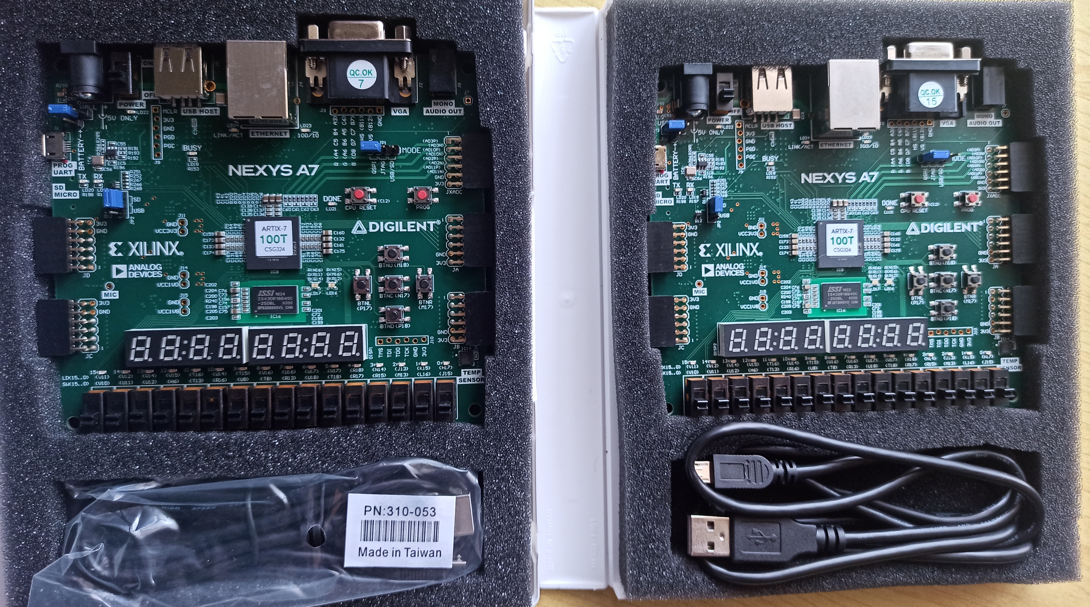
3 | Nexys Boards |
Chips to Startup (C2S) Programme
B V Raju Institute of Technology, Narsapur
OVERVIEW
The vision of Honorable Prime Minister of India, Shri Narendra Modi, to foster next-generation capabilities among chip designers is being actively realized through the Chips to Startup (C2S) Programme. This initiative aims to train 85,000 specialized professionals over a period of five years in the domains of VLSI and Embedded System Design, thereby strengthening India’s Electronics System Design and Manufacturing (ESDM) ecosystem. In alignment with this vision, B V Raju Institute of Technology, Narsapur, has been empowered under the C2S program with access to advanced Electronic Design Automation (EDA) tools and cutting-edge infrastructure, enabling high-quality education, research, and innovation in semiconductor design. Furthermore, this initiative is strongly supported by the India Semiconductor Mission, which aims to build a robust semiconductor and display ecosystem in the country. Together, these efforts are accelerating the development of skilled manpower, promoting indigenous chip design capabilities, and positioning India as a global hub for semiconductor innovation and self-reliance.
S.No | Tool Description | Name of the EDA tool |
1 | Frontend and Backend Design Tools, Analog IC Design Tools | Synopsys |
2 | Frontend and Backend Design Tools, Analog IC Design Tools | Cadence |
3 | Frontend and Backend Design Tools, Analog IC Design Tools | Siemens |
4 | Advanced Design System | Keysight |
5 | HFSS, Q3D | Ansys |
6 | TCAD | Synopsys |
7 | Silvaco TCAD | Silvaco |
8 | Renesys Embedded Softwares | Renesys |
INVESTIGATORS
Principal Investigator (PI): Dr. U. Gnaneshwara Chary
Co-Principal Investigator (Co-PI): Dr. Madhava Rao
ACTIVITIES CONDUCTED IN THIS PROGRAMME
- Set up state-of-the-art EDA labs to facilitate advanced chip design and research
- Delivered Faculty Development Programs (FDPs) and technical training sessions
for skill enhancement .
- Conducted workshops and seminars in VLSI and emerging technologies
- Implemented FPGA-based projects to provide practical design experience to students
- Produced research publications and filed patents in relevant domains
- Encouraged startup and incubation activities to foster innovation
- Built strong industry partnerships and internship programs to enhance
real-world exposure.
Major Project (IV year Students):
| S.No | project batch number | Roll number | Name of the Student | Guide Name | Project title |
| 1 | ECE_CVD_01 | 22211A0409 | Ananya Moturi | Mr. U Gnaneshwara Chary | Design and Analysis of EMI in Flip Chip Ball Grid Array |
| 2 | 22211A0438 | Bolleddu Sravanthi | |||
| 3 | 22211A0452 | Chowki Vinuthna | |||
| 4 | 22211A0458 | Vijaya Kaivalya Lahari Datla | |||
| 5 | ECE_CVD_02 | 23215A0401 | Amudala Mounika | Mrs. Vandana Ch | Development of Plant Growth Monitor in Agriculture using RISC V |
| 6 | 23215A0402 | Badam Akshari Srikari | |||
| 7 | 23215A0404 | Bussa Shruthi | |||
| 23215A0406 | Sravani Damera | ||||
| 8 | ECE_CVD_03 | 22211A0414 | Arraram Varsha | Dr. Pavan Kumar Bikki | Design of Low power PCIe 5.0 Protocol Interface with FIFO and CRC Support |
| 9 | 22211A0446 | Ch.Niharika | |||
| 10 | 22211A0460 | Dhanavath Bhaskar | |||
| 11 | 23215A0403 | B.Pavan Sai | |||
| 12 | ECE_CVD_04 | 22211A0480 | G.Renuka | Mr. C Ramesh Kumar Reddy | Optimized QPSK Modem on FPGA with Clock Gating and ROM-Based Signal Generation |
| 13 | 22211A0488 | Jatothu Akhil Kumar | |||
| 14 | 22211A0485 | Ivatury Harshita | |||
| 15 | 22211A04A0 | Kancharla Ananya | |||
| 16 | ECE_CVD_05 | 22211A04A3 | K Subramanya Pavan Kumar | Mrs. Vandana Ch | Algorithm-Level Error Detection in Low-Voltage Systolic Arrays |
| 17 | 22211A04B7 | K .Uday Kiran | |||
| 20 | ECE_CVD_06 | 22211A04B9 | Krupalaxmi | Dr. Pavan Kumar | Design and Implementation of Low Power Digital FIR Filter for ECG signal denoising |
| 21 | 22211A04C0 | K Vinay Reddy | |||
| 22 | 22211A04C1 | K Alekhya | |||
| 23 | 23215A0415 | Konda Chaitrika | |||
| 24 | ECE_CVD_07 | 22211A04D8 | M. Durgaa Sravani | Mr. C Ramesh Kumar Reddy | Real time Image Processing system for Imaging Applications on the PYNQ-Z2 Board |
| 25 | 23215A0416 | Kotala Sandeep Kumar | |||
| 26 | 22211A04E1 | M.Hrushikesh Reddy | |||
| 27 | 22211A04G5 | N.Jairam | |||
| 28 | ECE_CVD_08 | 22211A04G6 | Nakkirtha Amulya | Dr. K Madhava Rao | Low Power Video Processing Accelerator with RISC – V Core |
| 29 | 22211A04H1 | P S Mohith Varma | |||
| 30 | 22211A04H7 | Patimidi Amritha Reddy | |||
| 31 | 22211A04J8 | Rishitha Pragada | |||
| 32 | ECE_CVD_09 | 22211A04C9 | Sai Koushik Kovuru | Mr. U Gnaneshwara Chary | Low Power ASIC design for Glucose Level Trend Monitoring |
| 33 | 22211A04D2 | K.Rohith | |||
| 34 | 22211A04E5 | Mannelikar Revanth Kumar | |||
| 35 | 22211A04J7 | Pottipochala Prudula Sai | |||
| 36 | ECE_CVD_10 | 22211A04K4 | Ranaveni Saikiran | Dr. K Madhava Rao | VLSI Based Proximity Warning System For Mobile Vehicles |
| 37 | 22211A04L0 | Rohith Kongara | |||
| 38 | 22211A04L2 | Sai Datta Charan Parasa | |||
| 39 | 22211A04N6 | Snehansh Dubey | |||
| 32 | ECE_CVD_11 | 22211A04M6 | Sheikh Ishrathunnisa | Mrs. Vandana Ch | Strategic Sector Innovation in Object Detection |
| 33 | 22211A04P4 | Sreeja Thavidishetty | |||
| 34 | 23215A0424 | Naga Laxmi | |||
| 35 | 22211A04A6 | Sreeja Karnati | |||
| 36 | ECE_CVD_12 | 22211A04L6 | Manikanta Samineni | Mr. K Charan Kumar | Smart Biometric Door Lock using Verilog and Machine Learning Algorithms |
| 37 | 22211A04N7 | Sanjana Sriram | |||
| 38 | 22211A0495 | K. Harshavardhan Reddy | |||
| 39 | 22211A0497 | Kallepally Srinitha |
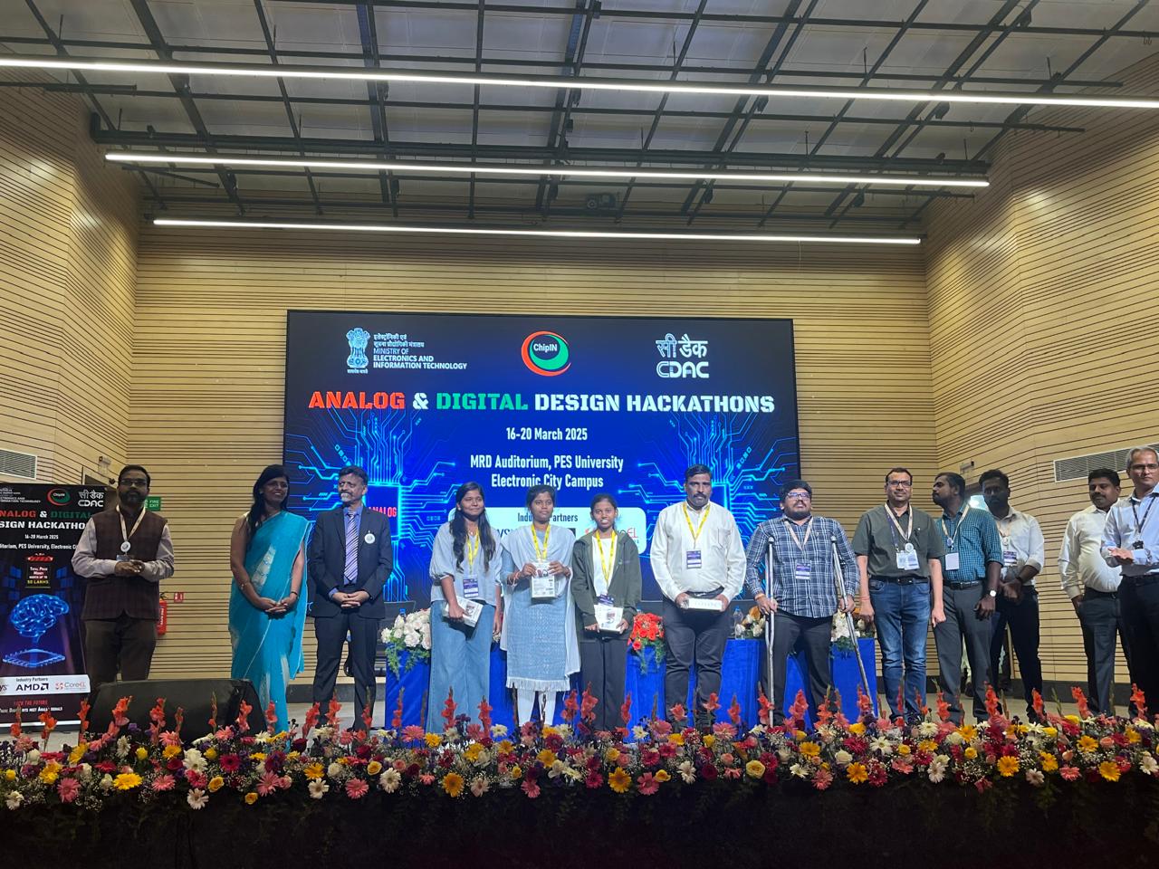
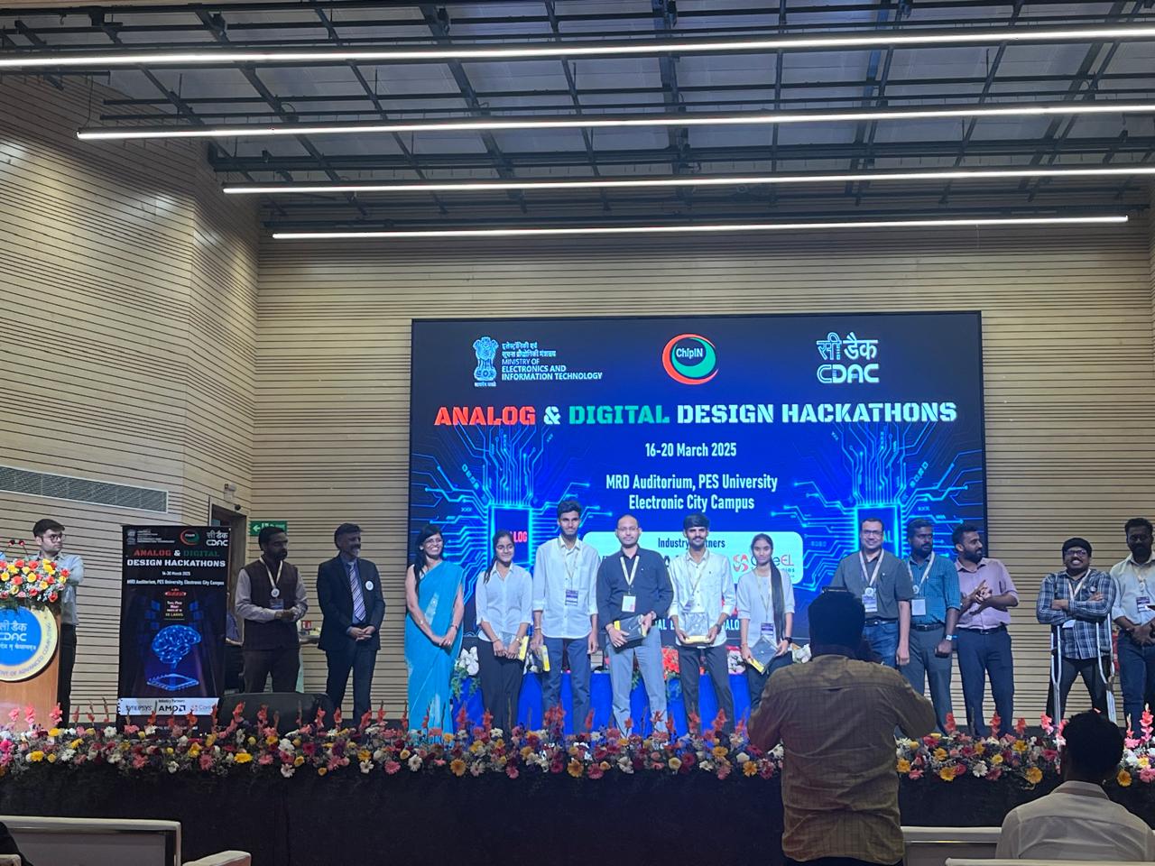
Analog & Digital Design Hackathon
Congratulations to both teams from BVRIT, Narsapur for making it to the final round of the Analog & Digital Hackathon conducted by ChipIN Team under the C2S Program, CDAC Bangalore!
Being among the top 20 teams across India is a remarkable achievement, and securing consolation prizes for both teams is truly commendable!